Packaging and assembly technologies are fundamental to make the results of advanced photonic research practically usable. At present advanced photonic packaging technologies are not easily available and a historically weak or not coherent effort in developing such technologies has created what is nowadays a clear major bottleneck for the future commercial exploitation of photonic devices.
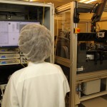
The advanced packaging platform aims to support and develop back end and packaging technologies, starting from package design, process development up to engineering and prototyping. A complete operative pilot line is able to support prototyping and small/medium productions up to thousands/year fully packaged components.
Objectives for the platform are:
- to give packaging support for the overall photonics community, including sensors and MEMS based solutions
- to facilitate access to customers asking for packaging developments
- to offer best packaging solution and designs based on consideration of the whole picture
- to offer prototyping up to small volume productions to SME and big industries using an automated pilot line
Main equipment includes:
- Automatic die-attach FINETECH model PICO
- Automatic ball wire bonder K&S
- Manual wire bonder TPT model HB16
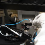
- Automatic multipurpose Alignment and Pigtailing Bench
- Flip-Chip technology with submicron tolerances, laser assisted, 12” wafer capability
- Reflow/Vacuum Chamber
- Vision microscopy
Main technologies include:
- Die bonding, Flip Chip BondingTacking, In situ reflow, Eutectic Bonding
- Epoxy bonding, Glob Top
- Wire bonding, Ribbon bonding
- Vertical and Horizontal Alignment and Pigtailing for silicon photonics devices, fiber arrays, laser subassemblies, lenses
- RF applications
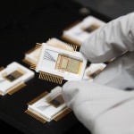
- Chip on board
- 3D stacking
In particular a unique and innovative automatic bench for silicon photonics applications, that includes the pigtailing of fiber arrays as well of active devices (laser pill/Laser micropackage) has been designed and realized.


