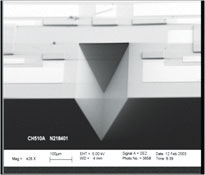
The “Hybrid Integration” Platform aims to develop technologies that can fulfill the necessity to integrate different devices and parts together, supporting packaging activities in the realization of structures, enabling compactness and interoperability. In particular the platform will develop the use of micro-structured silicon as the “silicon optical bench” (SiOB).
SiOB generally defines the technology in which active and passive optoelectronic components are assembled on a silicon micro machined chip.
Optical components based on SiOB are cost effective when compared to discrete optical elements, in particular considering the increase of an optical subsystem complexity.
The common technology used to achieve high accuracy position of discrete elements is the “silicon wet anisotropic etching”.
The anisotropic etching defines structure with high accuracy position (<±1.5μm in XYZ) related to silicon crystal plane {111} on a silicon wafer (100); an example of structure that could be used for high accuracy position is the so called V-groove structure, featuring an angle of 54° suitable for fiber, lens or other discrete component position. Another significant structure for this application is the so-called turning mirror at 45° that allows turning the light direction from horizontal to vertical orientation.
 The aforementioned technology, based on 6” wafer, is a controlled etching with strong basic chemical components like KOH or TMAH (tetramethyl ammoniumhidroxide) performed in a dedicated reactor.
The deposition of proper metal layers for electrical signal interconnection and the availability of the eutectic alloy Au-Sn 80/20 deposition technology (for laser diode or general solder attachment) allows complete manufacturing of a SiOB.
